The aim of the workshop is to bring together researchers working in the field of magnetic devices and related materials to stimulate new ideas and directions in emerging applications in biomagnetism. This event is organized in the framework of the OXiNEMS project.

Attendance to this event is free-of-charge upon registration

When? Tuesday April 16th, 2024
Where? Online (platform and link will be communicated to registered participants)

Updates will be notified on X (Twitter) @OXiNEMS_Project


 Program (The times indicated refer to the UTC+2 zone, Central European Summer Time)

12:30 Openings - Luca Pellegrino (CNR-SPIN, Italy)

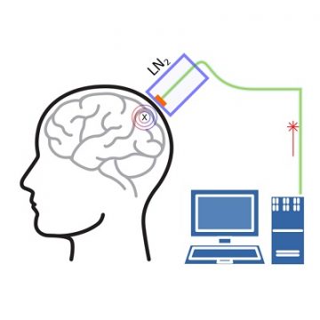
12:45 New trends in MEG instrumentation: why we need new generations of magnetometers? - Stefania Della Penna  (G. D’Annunzio University of Chieti and Pescara, Italy)

13:30 Colour centres for magnetometry in bio- and life-sciences - Ilia Breev (Technical University of Denmark (DTU), Denmark)

14:00 Frequency modulated MEMS magnetometer using integrated permanent magnets and magnetic flux concentrators Federico Maspero  (Politecnico di Milano, Italy)

14:30 - 15:00 COFFEE BREAK

15:00 Recent advances in modeling ∆E-effect magnetic field sensors - Benjamin Spetzler (Technische Universität Ilmenau, Germany)

15:30 Controlling the Magnetoresistance of EMR Devices in High Mobility Materials - Thierry Désiré Pomar (Technical University of Denmark (DTU), Denmark)

16:00 Evolving Magnetoelectric Field Sensing from Magnetostrictive Composites  - Lukas Zimoch (University of Kiel, Germany)

16:30 The OXiNEMS project: results and perspectives  - Luca Pellegrino (CNR-SPIN, Italy)

17:00 Discussions and closing remarks


Our M/NEMS devices are based on suspended and moveable structures. Generally, we start from an oxide thin film deposited on an oxide substrate by Pulsed Laser Deposition and prepare a photoresist mask using common photolithographic techniques such as optical lithography. We transfer the photoresist pattern to the film using physical or chemical etching. Physical etching is performed by ion milling technique: energetic Ar ions bombard onto the surface of the sample and progressively remove the oxide film areas that are not covered by the photoresist. Photoresist is removed by Ar ions too, but its thickness (about 4 microns) is higher than that of the film (about 0.1 microns). After the milling process, we remove the photoresist mask by solvents, leaving its replica onto the oxide film. Part of the substrate can be also removed during this process depending on the duration of the ion milling process. Ion milling is not selective and it removes all the materials, each one with different specific rates. Oxide films can be also etched by chemical methods; each composition has its own recipe. Prolonged wet etching may cause the etching of the film below the photoresist mask.

Regarding the suspension or release process, the removal of the oxide substrate regions under the patterned film is made using wet chemical etching. To do so, we explore the different sensitivity of oxides to chemicals. A typical example is that of manganite ((La,Sr)MnO3) thin films grown on strontium titanate (SrTiO3) substrates: a HF:H2O solution removes SrTiO3, while it does not affect (La,Sr)MnO3. A patterned (La,Sr)MnO3 microbridge can be made freestanding by prolonged immersion in HF:H2O solution, because the acid progressively removes the portions of SrTiO3 under the manganite pattern. Instead, HCl:H2O solution removes (La,Sr)MnO3 but not SrTiO3; (La,Sr)MnO3 sacrificial layers can be thus employed to fabricate freestanding SrTiO3 thin film structures by prolonged immersion in HCl by patterning SrTiO3/(La,Sr)MnO3 thin film heterostructures (see also L. Pellegrino et al. Adv. Mater. 2009, 21, 2377–2381). After chemical etching, the devices are rinsed in water and dried using Critical Point Drying method to avoid stiction.

In OXiNEMS, we study the etching protocols of selected oxide thin films for the realization of different classes of M/NEMS structures having moveable elements.

back to Outreach

Oxide films are made by Pulsed Laser Deposition, a versatile physical vapor deposition technique commonly employed for the fabrication of complex oxide thin films. The general principle of PLD is quite simple: a high-power pulsed laser beam (usually an excimer laser) is focused to a pellet (target) of the desired material located in a vacuum chamber. The laser beam evaporates ions, neutral atoms and species from the target in what is said “the ablation-plume”. In front of the target, at about 50 mm, is located a substrate where a film made of the elements and stoichiometry contained the target itself starts to grow. Composition of the target material is usually that of the wanted phase, but off-stoichiometric targets are sometimes prepared to compensate for evaporation of high volatility elements or resputtering from the film surface. The typical film grow rates are in the 0.01 nm/laser pulse range, about 100 nm/hour for a 3Hz pulse repetition rate. Good film crystal quality is achieved by tuning the different growth parameters. For example the substrate temperature, which is typically of few hundreds of degrees Celsius, the oxygen pressure in the chamber (for oxides growth), usually between 1 mbar and 10-6 mbar, the intensity of the laser, that can reach several hundreds of milliJoules per pulse, equivalent to few MW of power (the laser pulse duration is about 20 ns). Target-to-substrate temperature is also an important parameter to consider when depositing films by PLD.

back to Outreach

Project coordination

Luca Pellegrino – National Research Council
CNR-SPIN, Corso Perrone 24- 16152 Genova (Italy)
Tel: +39-010-6598751
This email address is being protected from spambots. You need JavaScript enabled to view it.


Administrative, Financial and Legal Management

Barbara Cagnana - National Research Council
Corso Perrone 24- 16152 Genova (Italy)
Tel: +39-010-6598723
This email address is being protected from spambots. You need JavaScript enabled to view it.


Follow us on social media

Twitter  


Page 1 of 2